Chainable LED Matrix Displays
General Description
S.1
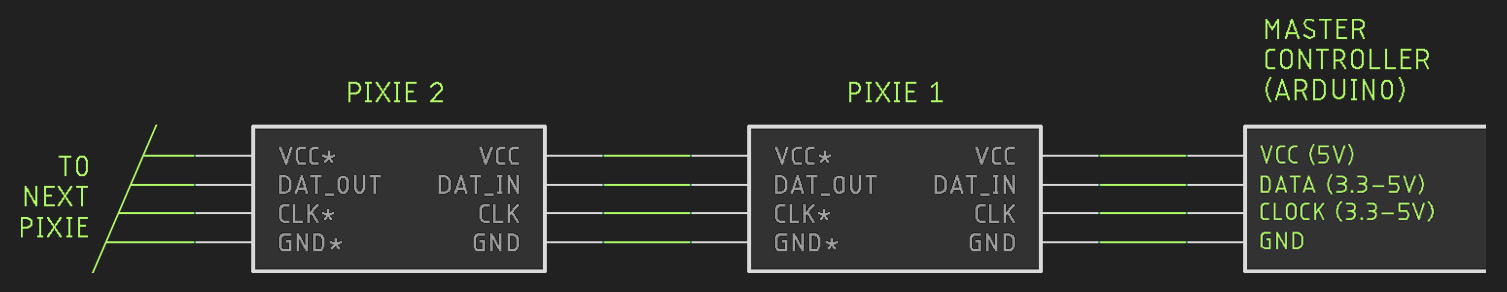
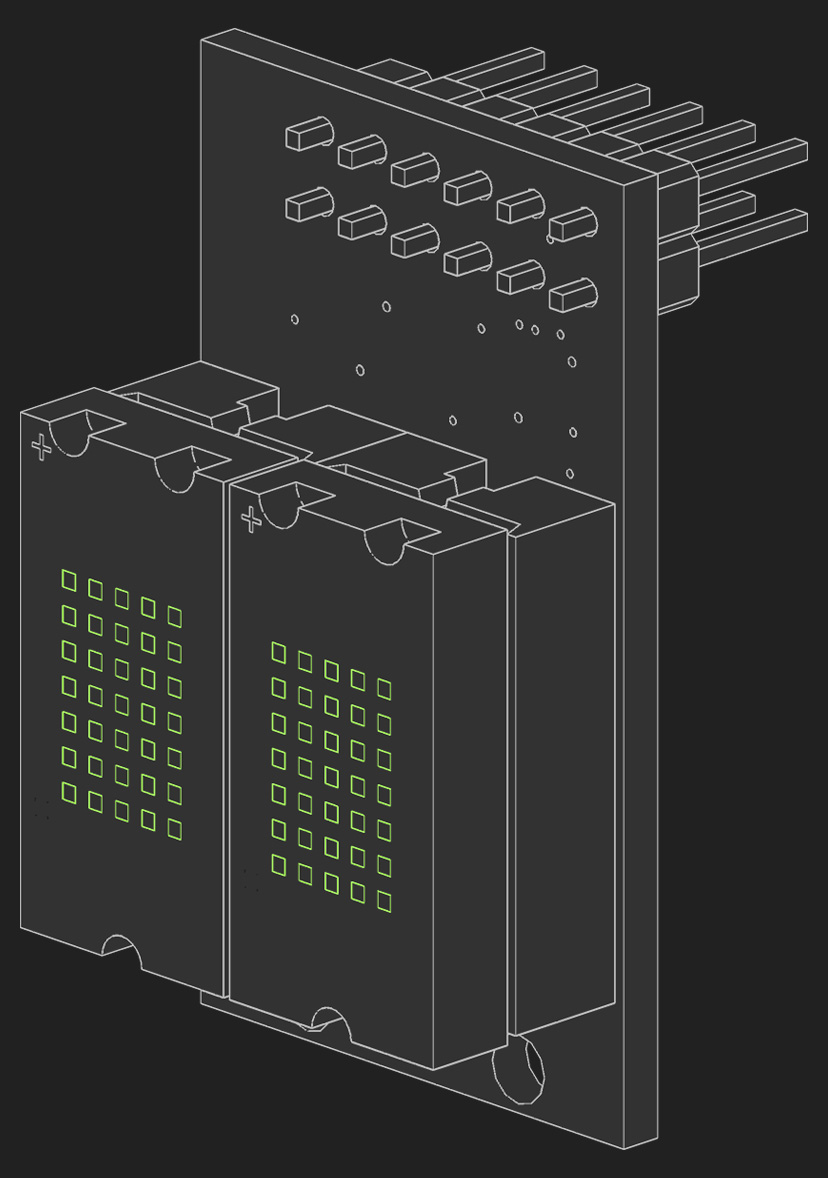
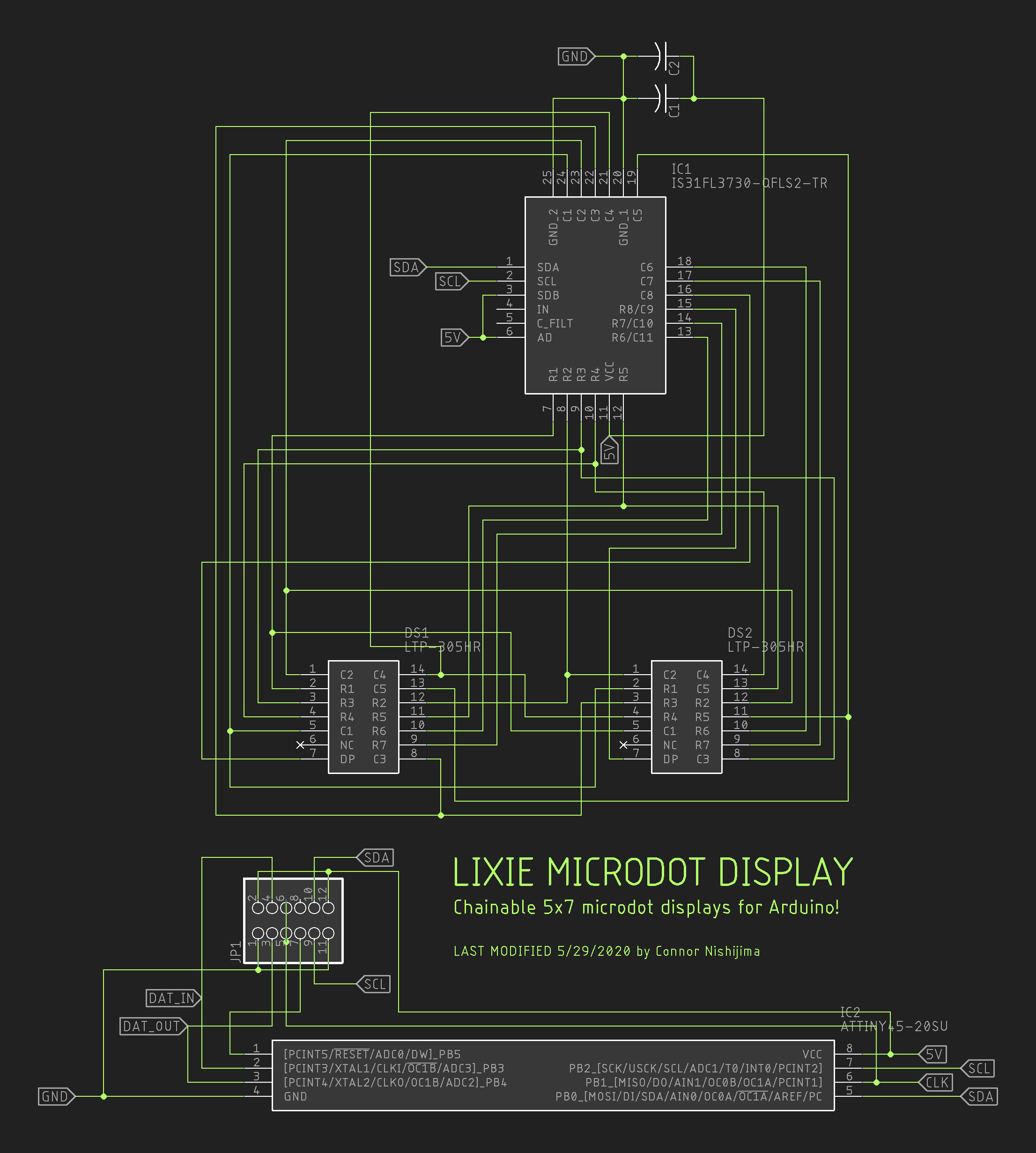
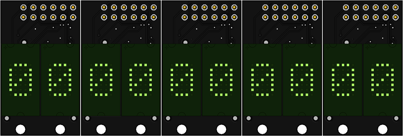
PIXIE is a compact, chainable, (Figure 1) dual 5x7 LED dot-matrix display platform (compatible with Arduino) that offers full bitmap control with 7-bit global PWM and high refresh rates.
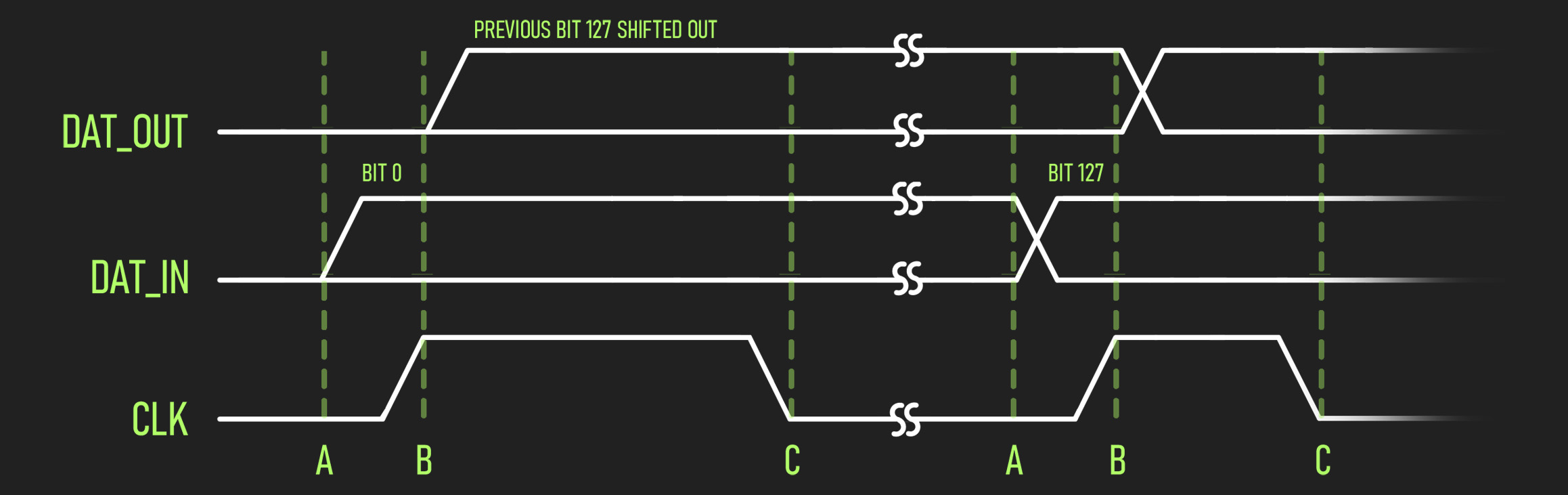
Using only two GPIO for DATA and CLOCK, bits can be simultaneously shifted in and out of each PIXIE at 39KHz (LEGACY_SPEED) or 67kHz (FULL_SPEED) (Note 7) (Figure 2) Final frame rate depends on the number of displays in the chain. For example - assuming a 67kHz clock speed:
| Character / Display Count |
Frame Rate |
| 2 - (1 PIXIE) |
~145 |
| 4 - (2 PIXIES) |
~113 |
| 6 - (3 PIXIES) |
~93 |
| 8 - (4 PIXIES) |
~79 |
| 12 - (6 PIXIES) |
~61 |
| 24 - (12 PIXIES) |
~36 |
After 3
ms since the last clock pulse was receieved, the internal 16-byte display buffer is latched and sent to the on-board IS31FL3730 driver over I
2C to update the PIXIE's displays.
(Figure 3)
Features
S.2
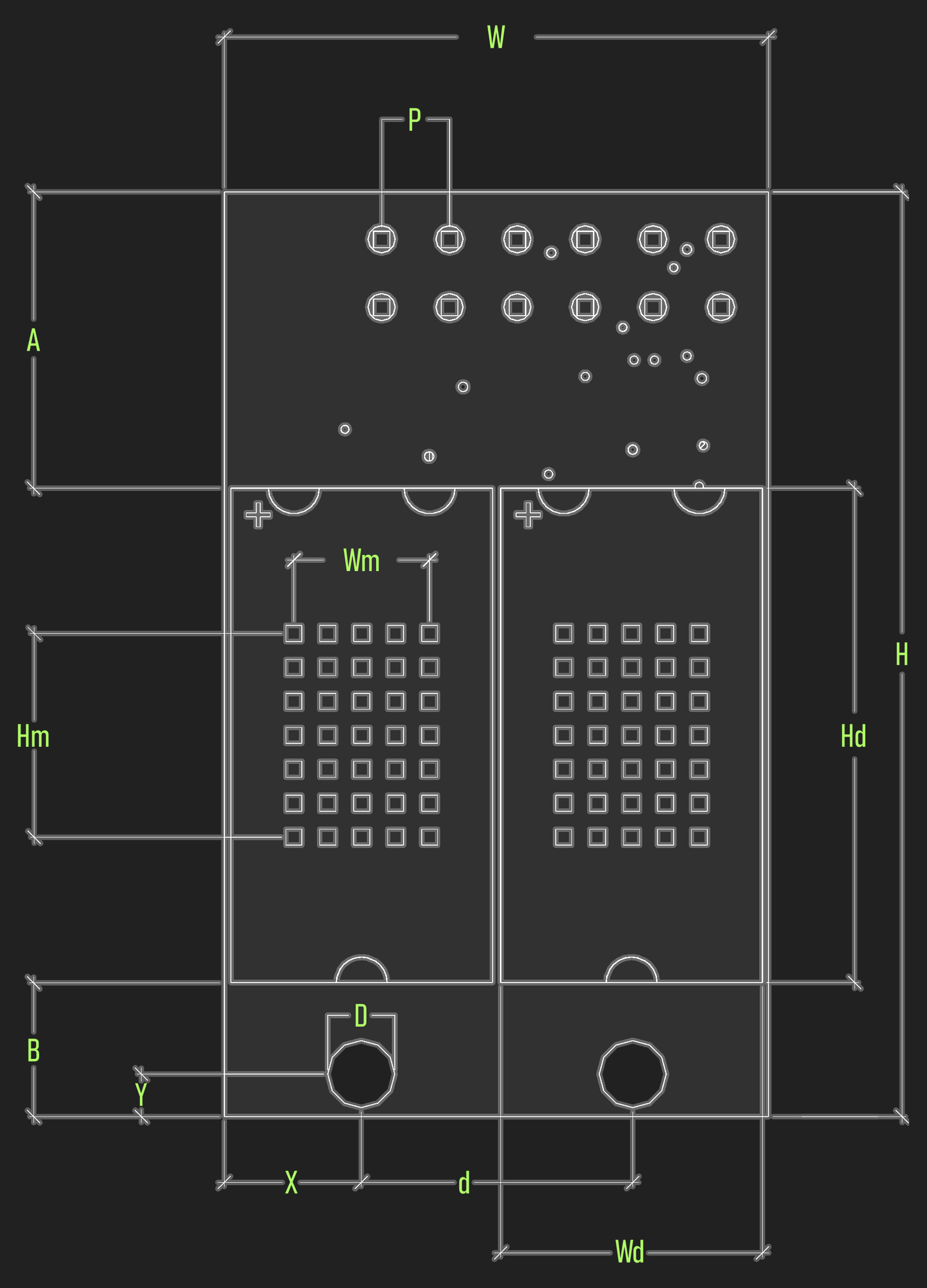
- Dual 5x7 LED matrices (Figure 4)
- 2.7V to 5.5V supply
- Fast bitmap control
- 7-bit global PWM (128 brightness levels)
- Over-temperature protection
- Resettable from controlling device
- Reprogrammable ATTINY45 microcontroller
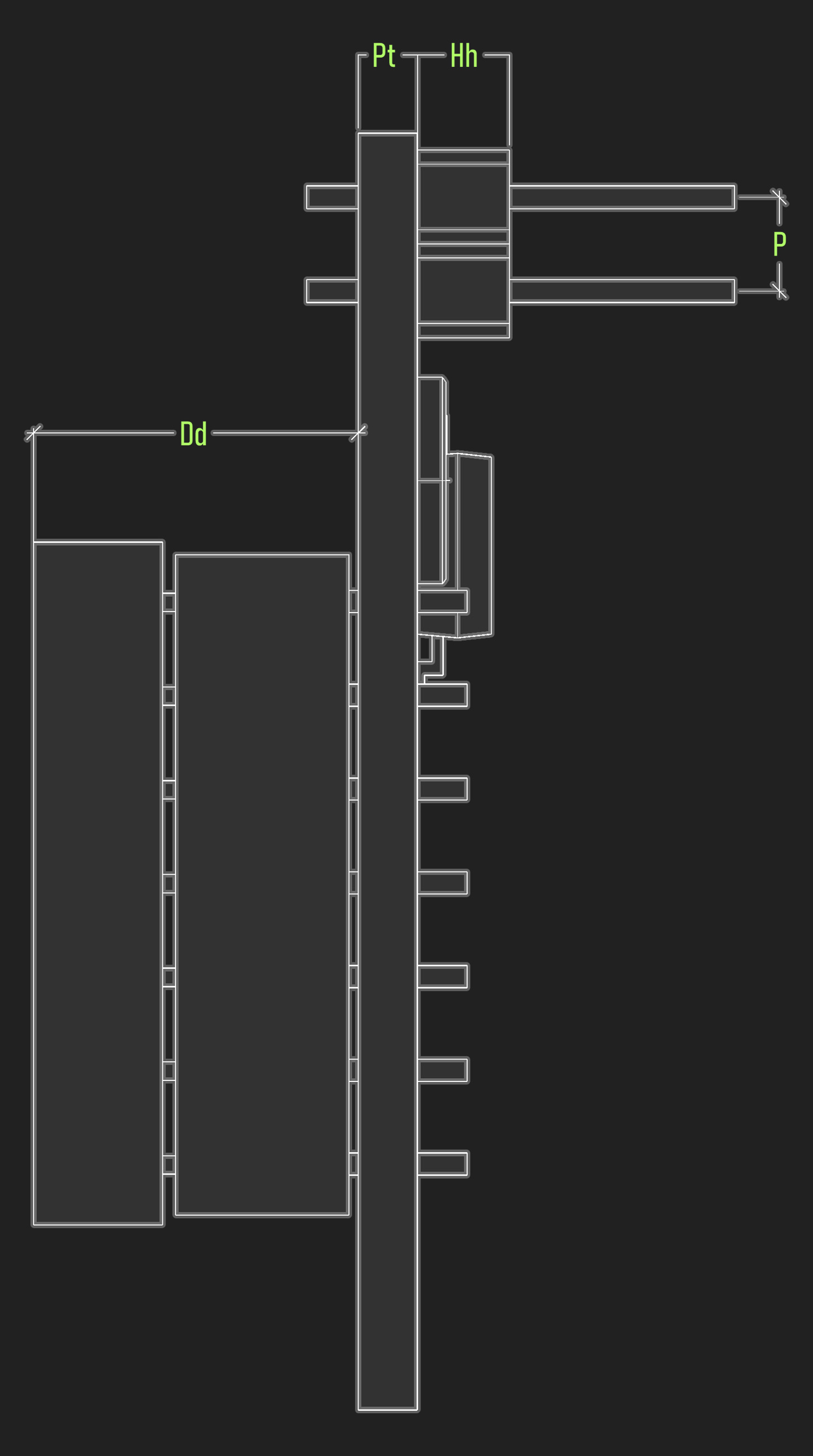
- 5.1mm * 7.6mm matrix size (19.92 ppi)
- 20.6mm * 34.7mm package
- M2.5 mouting holes
Applications
S.3
- Time-keeping
- Stock tracking
- Analytics
- Notifications
- Signage
- Point of Sale
Internal Devices
S.4
- ATTINY45 microcontroller
- IS31FL3730 LED matrix driver
- LTP-305G/HR 5x7 matrices
Pin Configuration
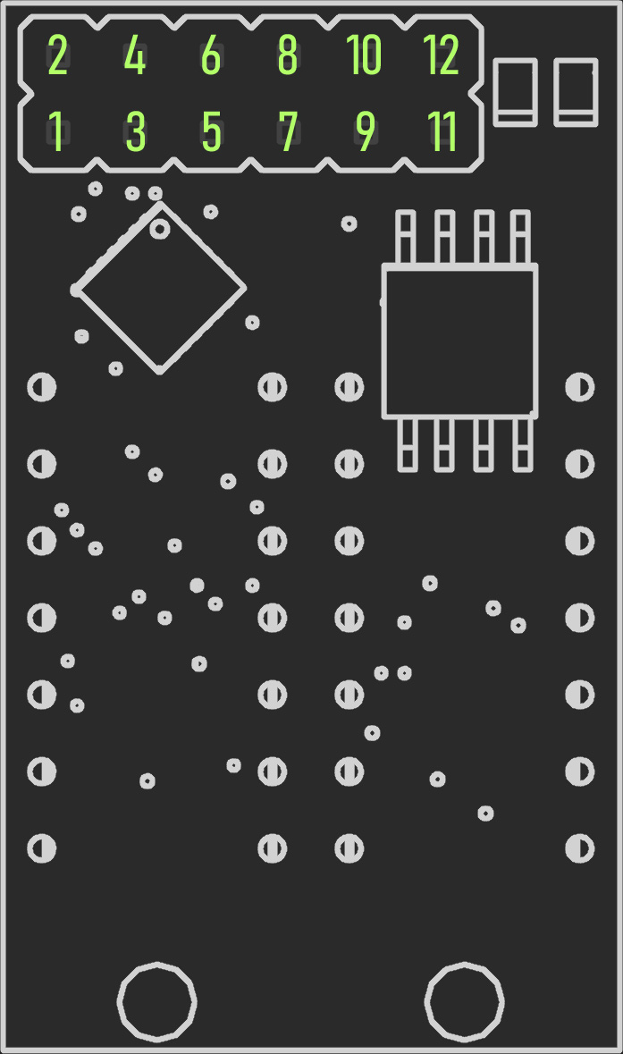
| Pin |
Number |
Function |
| GND |
1 |
Ground / Common (ATTINY / IS31FL3730 GND) |
| VCC |
2 |
Power Supply (ATTINY / IS31FL3730 VCC) |
| DAT_OUT |
3 |
Bitmap data OUTPUT |
| DAT_IN |
4 |
Bitmap data INPUT, no pullup (Note 1) |
| CLK |
5 |
Bitmap clock INPUT, no pullup (Note 1) (ATTINY MISO) |
| CLK* |
6 |
(Same as above) |
| RESET |
7 |
(ATTINY RESET) |
| NC |
8 |
(Not Connected) |
| SCL |
9 |
(IS31FL3730 I2C SCL line / ATTINY SCK) |
| SDA |
10 |
(IS31FL3730 I2C SDA line / ATTINY MOSI) |
| GND* |
11 |
(Same as above) |
| VCC* |
12 |
(Same as above) |
NOTE 1: DAT_IN and
CLK are INPUTS
without pullups. This is done to prevent damage in the scenario that a PIXIE is powered with 5V on V
cc but is receiving data from 3.3V-tolerant pins.
(i.e. ESP8266 / 32 / Teensy) The master controller must drive these pins both
HIGH and
LOW and not release these floating pins.
Typical Application Circuit
S.5
Absolute Maximum Ratings
| Supply voltage, VCC |
-0.3V ~ +6.0V |
| Storage Temperature Range |
-40°C ~ +85°C |
| Operating Temperature Range |
-40°C ~ +85°C |
NOTE 2: Stresses beyond those listed under “Absolute Maximum Ratings” may cause permanent damage to the device. These are stress ratings only and functional operation of the device at these or any other condition beyond those indicated in the operational sections of the specifications is not implied. Exposure to absolute maximum rating conditions for extended periods may affect device reliability.
Electrical Characteristics
S.6
| Parameter |
Condition |
Min. |
Typ. |
Max. |
Units |
| Supply Voltage (Vcc) |
(Note 2) |
2.7 |
5.0 |
5.5 |
V |
| Matrix Output Current |
|
|
40 |
|
mA |
| Peak Emission Wavelength (Green) |
|
|
565 |
|
nm |
| Peak Emission Wavelength (Red) |
|
|
635 |
|
nm |
Digital Input Switching Characteristics
S.7
| Parameter |
Condition |
Min. |
Typ. |
Max. |
Units |
| DATA CLOCK frequency |
(Note 3) |
39.0 |
39.0 |
67.0 |
kHz |
| DATA CLOCK LOW time for display latch |
|
3 |
5 |
|
milliseconds |
| DATA CLOCK HIGH time for reset |
|
10 |
|
|
milliseconds |
| Minimum TTL Logical "1" Level (HIGH) |
(Note 4) |
Vcc * 0.52 |
Vcc |
Vcc |
V |
| Maximum TTL Logical "0" Level (LOW) |
(Note 4) |
0V |
0V |
Vcc * 0.42 |
V |
NOTE 3: Max DATA CLOCK frequency depends on a minimum of 5V on Vcc. While it is possible to maintain the 16MHz clock of the ATTINY with only 3.3V on Vcc, this is not recommended or guaranteed.
NOTE 4: Due to the logic level
HIGH at 5V (on V
cc) being 2.6V, it is possible to control PIXIE with 3.3V TTL logic and a 5V power supply. (i.e. ESP8266 / 32 / Teensy) However, the PIXIE will output V
cc's voltage on the
DAT_OUT pin, regardless of the voltage sent to
DAT_IN /
CLK.
USAGE
DATA / CLOCK Interface
S.8
PIXIE uses a data / clock interface similar to SPI, but with a few distinctions:
- Uni-directional communication (One way - master controller to dependents)
- No "Chip Select" line (only one PIXIE chain per GPIO pair)
- Data is shifted OUT of the internal buffer on CLK HIGH transition, and read IN to the internal buffer on CLK LOW (Figure 2)
- Each PIXIE is the "master" to the next in the chain
The
CLK line is shared between all units in the chain, and each PIXIE's
DAT_OUT will connect to the next display's
DAT_IN.
(Figure 1)
The master controller controller
must drive the
CLK and
DAT_IN lines
HIGH and
LOW, and not release them at anytime, as these input pins
do not have pullup resistors attached/enabled.
(Note 1)
Once the
CLK line is
LOW and hasn't changed state in at least 3ms, the 128-bit display buffer is latched, and it's contents are parsed and sent over I
2C to the IS31FL3730 LED driver, updating the matrices.
In summary, the master controller must toggle the
DAT_IN line before each
HIGH CLK pulse, and the PIXIES in the chain will manage the passing of data before reading it on the
CLK LOW transition.
Reset Function
S.9
If the
CLK line is held
HIGH for more than 10ms (then set
LOW) the on-board ATTINY will reset to vector 0x0000 in ROM and reset the registers of the IS31FL3730 LED driver, blanking all displays in the chain.
Due to this, it's necessary to have the master controller keep the
CLK line
LOW when not in use.
| Marker |
Event |
| A |
DAT_IN State Change |
| B |
CLK rise, DAT_OUT set to last bit shifted out of current display buffer |
| C |
CLK fall, DAT_IN line read and bit written to 0th index of display buffer |
USAGE (CONTD.)
Internal Display Buffer
S.10
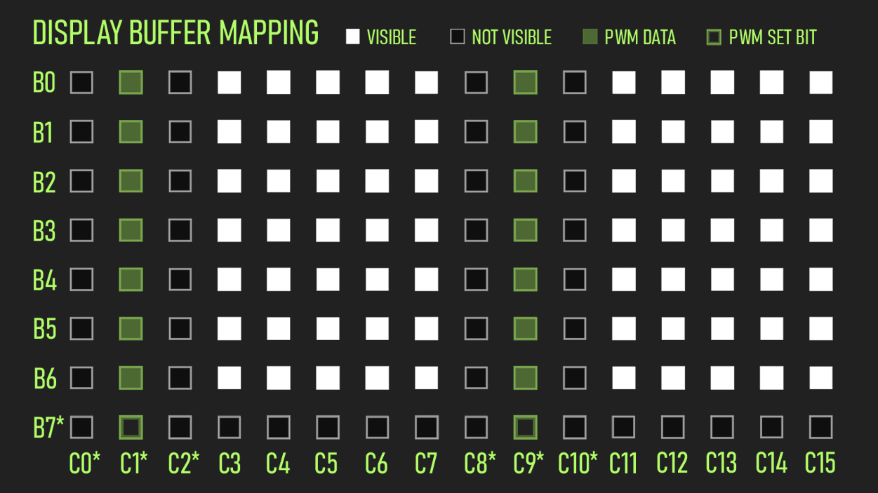
PIXIE has an internal 128-bit (16 byte) display buffer, parsed as a 16x8 matrix.
(Figure 3) The 5 columns C3-C7 pertain to the lefthand LED matrix, and C11-C15 are the righthand LED matrix.
*Some columns/bits in the buffer are not visible in the physical LED matrix, and are used as "dead space" for smooth scrolling across the gap between displays.
Columns C1 and C9 redundantly store the 7-bit PWM brightness of the PIXIE display in bits B0-B6. Only the PWM columns have B7 (MSB) set to 1, allowing the PIXIE to recognize and treat them as blank columns when scrolling them across the visible areas.
Some columns between visible displays are unused completely.
(Note 5)
SHIFTING DATA IN / OUT
S.11
When the
CLK line goes
HIGH, the bit at C0:B0 is set on the
DAT_OUT line, and the whole buffer is shifted left by one bit, overwriting the former value of C0:B0. (i.e. C0:B0 = C0:B1, C0:B7 = C1:B0, C15:B6 = C15:B7, etc.)
(Note 6)
(The output of C0:B0/
DAT_OUT will arrive at the
DAT_IN/C15:B7 of the next PIXIE in the chain.)
Next, when the
CLK line goes
LOW again, the logic level (0/1) of this PIXIE's
DAT_IN line is written to C15:B7.
Because of this bitwise shifting of the buffer, it is crucial that the master controller
sends a multiple of 128 bits every time the PIXIE chain is updated.
NOTE 5: Columns C0, C2, C8 and C10 are left blank, and are reserved for future development.
NOTE 6: In actuality, the buffer is not shifted in RAM, just a pointer for accessing it. (Circular buffer)
Revision History
| Revision |
Details |
Date |
| 1 |
Initial Release |
6/13/2020 |
| 1A |
Fixed Hole X Offset dimension error (Alex @tinyledmatrix) |
6/29/2020 |
| 1B |
Added reference to the 67kHz FULL_SPEED mode added in firmware version 1.1.0 (Note 7) |
7/3/2020 |